Vertically Coupling ZnO Nanorods onto MoS2 Flakes for Optical Gas Sensing
by
 , , , , and
Guido Faglia
1,2,* ,
,
Matteo Ferroni
1,3 ,
,
Thi Thanh Le Dang
1,4,
Maurizio Donarelli
1,5,
Federica Rigoni
1,6 and
Camilla Baratto
2 1
Università degli Studi di Brescia, Dipartimento di Ingegneria dell’Informazione, Via Branze 38, I-25123 Brescia, Italy
2
CNR-INO, Via Branze 45, 25123 Brescia, Italy
3
CNR-IMM Via Gobetti 101, I-40129 Bologna, Italy
4
ITIMS, Hanoi University of Science and Technology (HUST), Hanoi 100000, Vietnam
5
AQM srl, Via T.A. Edison 18, 25050 Provaglio d’Iseo (Brescia), Italy
6
Ca’ Foscari University of Venice, Department of Molecular Sciences and Nanosystems, via Torino 155/b, 30170 Venezia-Mestre, Italy
*
Author to whom correspondence should be addressed.
Chemosensors 2020, 8(1), 19; https://doi.org/10.3390/chemosensors8010019
Submission received: 16 January 2020
/
Revised: 19 February 2020
/
Accepted: 28 February 2020
/
Published: 2 March 2020
(This article belongs to the Collection Optical Chemosensors and Biosensors)
Abstract
:Hybrid structures composed of layered one-dimensional (1D) and two-dimensional (2D) materials opened new perspectives and opportunities through the build-up of hetero-junctions with versatile layered structures and led to fascinating fundamental phenomena and advanced devices. We succeeded in depositing by magnetron sputtering vertically aligned 1D ZnO nanorods on 2D MoS2 flakes obtained by exfoliation, preserving the structure of the 2D materials. The photoluminescence (PL) optical properties of the hybrid structure were assessed towards developing a contactless optical chemical sensor.

1. Introduction
Two-dimensional (2D) materials have received increasing attention due to their unusual electrical, optical, and mechanical characteristics; furthermore, coupling active one-dimensional (1D) and 2D materials is opening new and unexpected research scenarios and technological breakthroughs [1,2,3,4,5,6]. Although researchers are fascinated with graphene as compared to other 2D materials, the absence of a bandgap leads to its limited use in optical applications. Two-dimensional transition metal dichalcogenides (TMDCs), such as MoS2, WSe2, and WS2, are planar crystals made of one or a limited number of TMDC unit cells, possessing plentiful electronic, optical, mechanical, and chemical properties [7]. As for graphene [8], one can quickly obtain TMDC via the universally known ‘scotch tape’ mechanical exfoliation method [9,10]. Single-layered TMDCs are described by the formula MX2, where M is the transition metal from the fourth and tenth groups of the periodic table and X is a chalcogen (S, Se, or Te). Common polymorphs of TMDCs include trigonal 1T with one S-Mo-S sheet per unit cell, hexagonal 2H with two S-Mo-S sheets, and rhombohedral 3R with three S-Mo-S sheets per cell. Although TMDCs have been widely studied for decades, their role as near-atomically thin materials is new: some TMDCs, such as Mo and W dichalcogenide compounds, show indirect-to-direct bandgap transition when exfoliated from a layered bulk crystal to a single layer (for instance, MoS2 bandgap ranges from 1.3 eV, indirect, in the bulk phase, to 1.8 eV, direct, in the monolayer phase), drawing massive interest for applications in optical and photovoltaic devices. The direct bandgap also results in photoluminescence from monolayer MoS2, which opens the possibility of many optoelectronic applications [7]. In general, there are many interesting layer-dependent properties in 2D materials, including graphene and TMDCs, which differ significantly from the properties of the bulk materials.
The electronic, optoelectronic, and chemical properties of TMDCs make them very attractive in chemical sensing applications. As 2D materials, their high surface-to-volume ratio makes them particularly sensitive to changes in their surroundings. On exposure to gases and vapors, there can be changes such as charge transfer and doping, intercalation, and shifts in permittivity and lattice vibrations. Changes in the electronic properties of TMDCs caused by the presence of adsorbates have already been detected electrically by incorporating the TMDCs into transistor devices [11,12,13,14,15]. The detection mechanism is probably due to chemical doping induced by the adsorbed species as proposed for graphene [16], changing the resistivity of the intrinsically n-doped MoS2.
Optical readout-based contactless technology provides many benefits in respect to the traditional conductometric sensors, in particular when nanomaterials come into play, since the development of stable and reliable contacts for nanostructures is still a challenging issue. In addition, optical sensors do not suffer from electromagnetic noise and may allow optoelectronic integration. Sources may vary in intensity, wavelength, and polarization, and various optical responses may be detected, such as reflectance, optical absorption, surface plasmon resonances or photoluminescence (PL).
Metal oxide (MOX) nanowires (NWs), given their high degree of crystallinity and the high surface to volume ratio, exhibit PL emission in the visible region which is strongly related to the defect emission and in particular to oxygen vacancies. The PL spectra of ZnO thin films and nanostructures are typically composed by an UV peak due to excitonic recombination centered at a wavelength around 380 nm (and depending on nanostructure sizes [17]) and by a broad emission band in the visible range depending on deep defect states lying inside the bandgap. No shared consensus still exists concerning the origin of visible emission in ZnO: the green emission has been assigned to the transition between the photoexcited holes and single ionized oxygen vacancy [18], attributed to antisite oxygen [19] and donor-acceptor complexes [20,21]. Surface states have also been identified as a possible cause of the visible emission in ZnO NWs [22]. Additionally, the ratio of UV to visible emission is dependent on the preparation conditions [23].
In 2005, Faglia et al. [24] first demonstrated that the partial pressure of a gas species can be measured by monitoring the PL signal from SnO2 NWs, forming the basis for a new optical readout-based chemical sensor. NO2 at the ppm level quenched the spectral intensity of the PL emission band strongly by adsorbing over the surface and creating competitive non-radiative recombination paths. In the wake of the promising results obtained on SnO2, Faglia et al. [25] studied the room temperature continuous wave PL spectra of ZnO thin films and nanostructures: a low concentration of NO2 induced in ZnO a reversible quenching of both the excitonic and the visible band, and no peak shift. As happened to SnO2, the modifications in PL efficiency followed a non-linear dependence versus the gas concentration. Gas presence may affect PL quenching through two main mechanisms: the quencher gas molecules may either lower the probability of the photoexcitation process (static quenching) or contribute to a faster nonradiative decay of the photoexcited molecules (dynamic quenching). In the first case, the presence of the quencher molecules does not affect the single de-excitation process nor alters its decay time. Although the PL quenching of ZnO NWs by NO2 followed a Stern-Volmer model—supporting the model in which the quenching molecules act as dynamic quenchers—a clear sign of the static quenching was obtained by time-resolved PL measurements [26], which showed small modifications of recombination rates due to the introduction of NO2, not proportional to simultaneous changes in PL intensity. The effect of NO2 vanishes by increasing the temperature up to 220 °C. Indeed, at higher temperatures, the PL signal is also small due to increased thermal disorder. No response to CO, water vapor, and NH3 was recorded.
Hybrid structures composed of layered material opened new perspectives and opportunities through the construction of hetero-junctions with adaptable layered structures. One made of a 2D MoS2 flake obtained by exfoliation and a 1D ZnO NW array deposited by RT hydrothermal methods has been proposed for a pressure-gated FET (PGFET) [27]. A seed layer made by ZnO deposited by magnetron sputtering or Al2O3 by atomic layer deposition was patterned by electron beam litoghraphy (EBL) to enhance growth. For hydrogen photogeneration, ZnO nanostructures selectively grown by hydrothermal methods on an fluorine-doped tin oxide FTO glass (a 50 nm thick ZnO film by RF sputtering acting as seeds) were soaked into an ethanol solution where MoS2 powder was dispersed for 1 h to get a MoS2 nanosheet/ZnO NW hybrid nanostructures [28]. In optical applications, the antenna effect induced and enhanced PL and Raman emission in ZnO nanorods coupled to vapor-solid-growth MoS2 monolayers via the hydrothermal route [29]. In the chemical sensing field, a MoS2/ZnO p-n nano junction was proposed as a highly responsive and stable electrical sensor to NO2: MoS2 nanosheets with a vertically aligned structure were fabricated by sulfurization of direct-current (DC)-magnetic-sputtering Mo films on ZnO NWs; afterward, a hydrothermal reaction was utilized to synthesize ZnO NWs [30]. ZnO obtained by hydrothermal route was also mixed with a solution containing MoS2 nanosheets prepared by an ultrasonic cell crusher from bulk to produce an NO2 sensor [31]. In the biosensing field, a thin-layered MoS2 was prepared through an ultrasonic exfoliation method from bulk MoS2 and then the free-standing ZnO nanosheet was electrodeposited on the MoS2 scaffold for DNA sensing [32]. The free-standing ZnO/MoS2 nanosheets had a low detection limit and affected DNA immobilization and hybridization. As for bioactivity, a MoS2–ZnO nanocomposite synthesized by hydrothermal technique [33] showed selective cytotoxic activity against tumor cells.
Many approaches have been proposed to couple 2D MoS2 to 1D ZnO, leading to fascinating fundamental phenomena and advanced devices: the objective of this contribution is to study the PL optical properties for chemical sensing of a hybrid structure obtained by depositing ZnO nanorods through magnetron sputtering [34] on exfoliated MoS2 flakes, a process never yet carried out to the best of our knowledge.
2. Materials and Methods
MoS2 crystals were exfoliated in order to obtain few-layer (up to monolayer) molybdenite flakes. Several exfoliation techniques have been proposed in the last years, similar to the procedures previously introduced for the graphite exfoliation. The easiest way to obtain few and monolayer MoS2 flakes is the micromechanical exfoliation technique, using a conventional scotch tape [10]. This procedure allows one to obtain few microns squared multi and monolayer MoS2 flakes. MoS2 exfoliation was carried out as explained in [9]. The number of exfoliations was kept at a minimum in order to avoid a too significant decrease in the lateral size of the layers. Single- or few-layer MoS2 flakes were exfoliated from bulk MoS2 and directly attached to highly doped p-type silicon substrates covered with 100 nm thick SiO2, which provides excellent contrast for optical detection of MoS2 flakes [35].
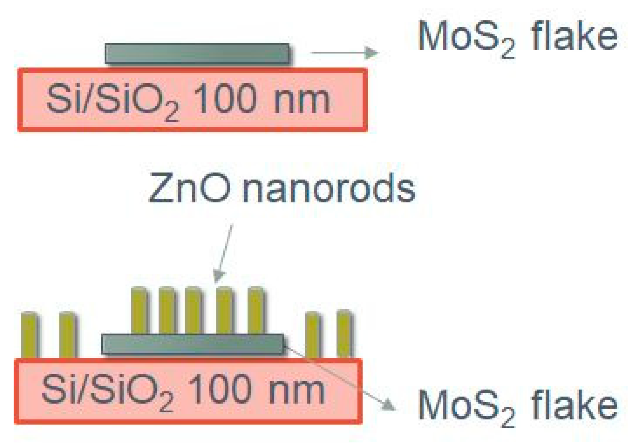
This work aimed to demonstrate that it is feasible to grow ZnO nanorods by RF sputtering on MoS2 without deterioration of the 2D material, as reported in Figure 1. To avoid damaging MoS2, the deposition should occur at temperatures lower than 300 °C, in order to avoid possible degradation or oxidation of the MoS2 flakes [36,37].
Sputtering deposition is a well-known, cost-effective technology that can be used in large scale plants, and foreseen for large scale integration. Competing techniques for ZnO NW growth include hydrothermal deposition, which involves water solution chemistry and is, therefore, less industrially scalable. We proved already that it is possible to deposit ZnO nanorods by RF sputtering, starting from Sn seeds at 400 °C [34]; deposition at a lower temperature was obtained starting from Cu rough layer [38], but involved a complex procedure for reaching proper Cu roughness. Physical deposition techniques, like growth by evaporation in furnaces, are not feasible due to the high-temperature process (600 °C) [39].
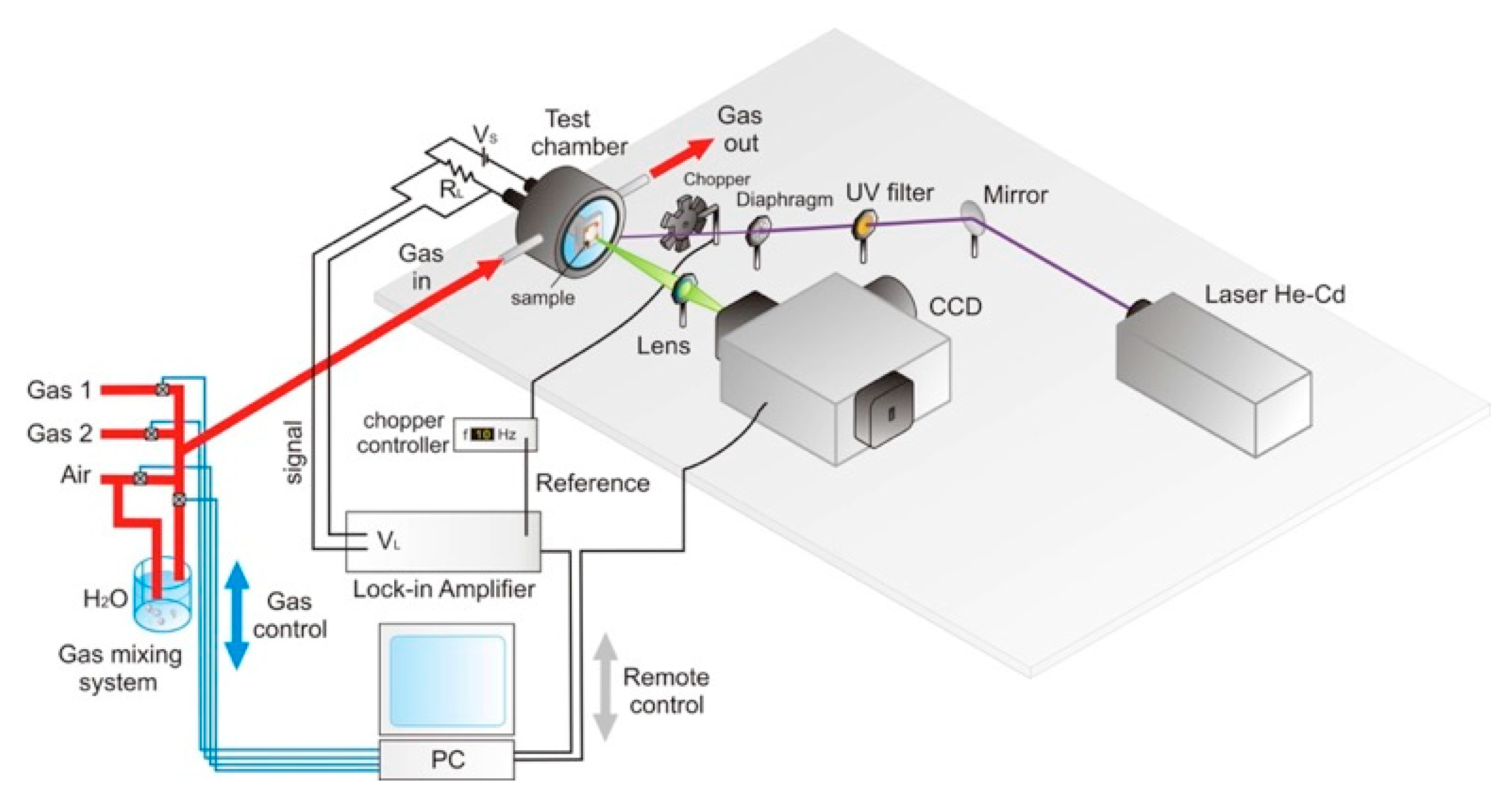
PL and Raman spectra were collected using a modular micro-Raman confocal system from Horiba equipped with a single grating monochromator and a Peltier-cooled charge-coupled device camera. As the excitation source, we employed a Kimmon IK5451RE solid-state laser at 325 nm (PL)/442 nm (Raman) wavelength with a nominal power of 10 mW/50 mW. A plano-convex lens (focal length 100 mm) and a set of UV neutral density filters decreased power density on the sample to avoid photobleaching along with interference filters on the laser lines and edge filters on the signal. The spectra were acquired perpendicular to the sample. Samples were mounted on an XY piezoelectric stage Märzhäuser Wetzlar Tango 3 model, which allowed steps of 100 nm. For Raman spectroscopy, we employed a 100X objective and 1800 l/mm grating. For PL spectroscopy, we employed a long working distance objective Zeiss 50X LWD coupled to a 600 l/mm grating to get, through a quartz window, inside a Linkam cell THMS600E allocating the samples, which can be cooled down to −196 °C and heated up to 600 °C, and has apertures for gas inlet and outlet.
PL gas sensing functional tests were carried out by the flow-through method: we set into the Linkam cell, at atmospheric pressure, a constant flux of humidified synthetic air equal to 0.1 l/min, mixed with the desired amount of NO2 diluted in air from a certified bottle (up to 10 ppm) in the working temperature from RT to 200 °C (see Figure 2). The spatial resolution of the experimental setup was diffraction-limited, and PL maps spectra were acquired at 0.5–2 μm steps of the motorized stage.
3. Results and Discussions
3.1. SEM Characterisation
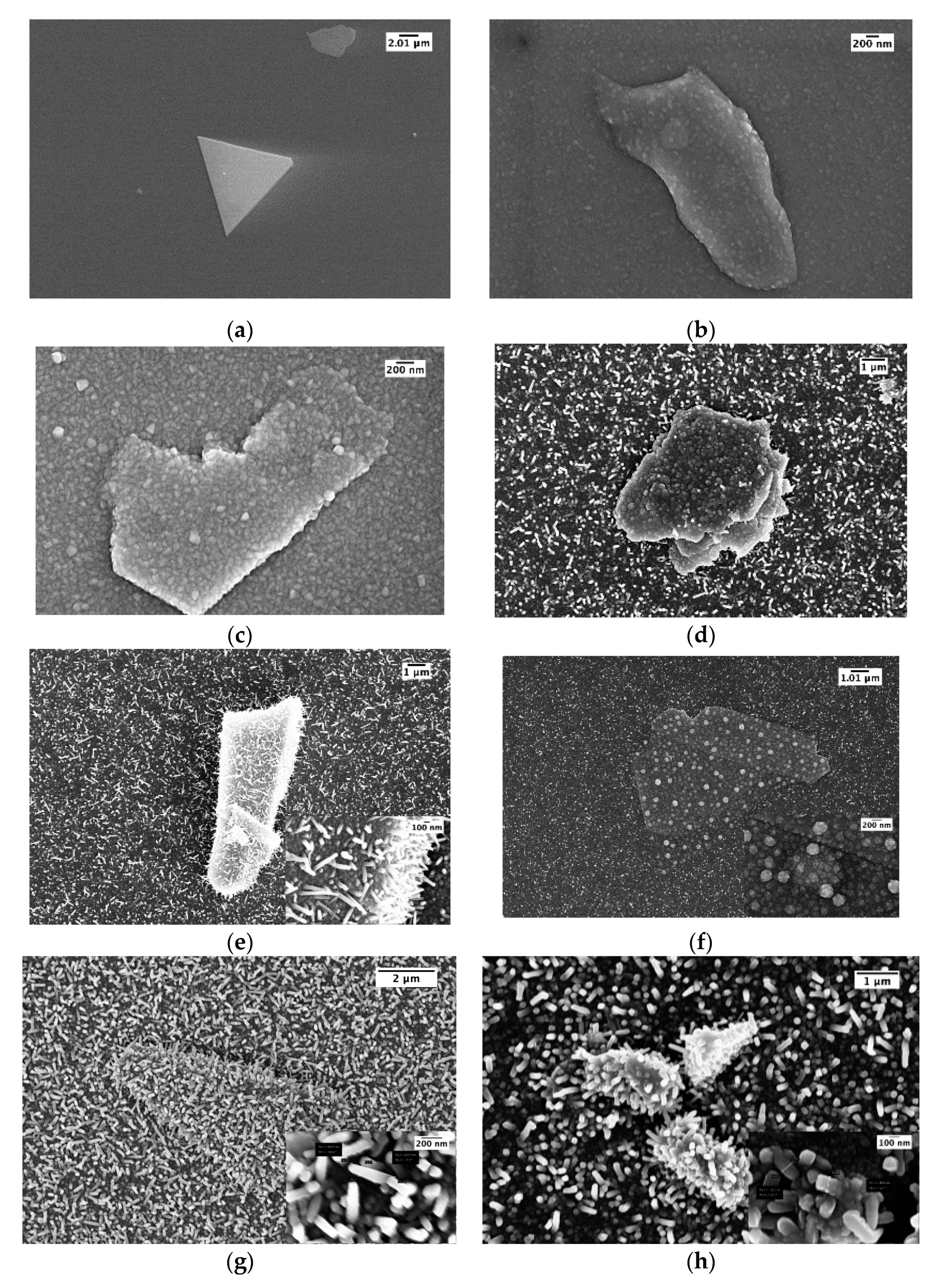
MoS2 was mechanically exfoliated onto SiO2 on a Si substrate, producing isolated flakes like the one shown in Figure 3a. The pictured specimen is an isosceles triangle with a side of 12 μm, but several smaller flakes are also visible all over the substrate. After inserting the sample into the sputtering plant, Sn was deposited first, keeping the substrate at a temperature ranging from 200 to 250 °C. The sputtering power and time for Sn were kept constant at 50 W and 5 s, respectively. The deposition of ZnO from an oxide target was carried out as the last step. We tailored the deposition of ZnO to substrate temperatures lower than 300 °C, in order to preserve the MoS2 structure.
Figure 3b–h show the morphology (SEM obtained) of the different samples we prepared and whose properties Table 1 summarizes.
The presence of the seed catalyzer is critical to induce columnar growth of ZnO at 200 °C Figure 3b and even at 400 °C. Introducing the Sn catalyzer at 200 °C, with the deposition temperature being near to the melting point (231.9 °C), tin droplet formation occurs, promoting columnar growth of ZnO, as can be seen in Figure 3c. In order to obtain nanorods, we further increased the substrate temperature to 250 °C: Figure 3d shows the presence of nanorods on the substrate and a columnar growth on the MoS2. As long as we obtained NW growth, in order to reduce the possible MoS2 damage due to the kinetic energy of the sputtered atoms, we reduced the deposition power from 200 to 150 and to 100 W. Figure 3e shows that NWs grow both on MoS2 and on a substrate at 150 W, but at 100 W only clustered ZnO grows on MoS2 (Figure 3f). At this stage, to improve the NWs density, we increased the deposition time to 10 and 15 min (Figure 3g,h, respectively), observing a dense growth of nanorods oriented in random direction in respect to the perpendicular to the substrate, with a diameter in the range of 80–100 nm for 10 min and 130–150 nm for 15 min deposition. The most effective sample was G, which was obtained at the lowest deposition power and with the smaller diameter of nanorods.
3.2. Raman and Photoluminescence PL Characterization
Raman spectroscopic studies were performed to evaluate the number of layers of the material and the potential damage induced by ZnO sputtering. In fact, the energy difference between the two Raman peaks E2g, which represents the in-plane vibrational mode of the Mo and S atoms, and A1g, which represents the out-of-plane vibrational mode of S atoms [40], can be used to identify the number of layers of the MoS2 flake under observation: a distance equal to 18 cm−1 is the fingerprint of a monolayer MoS2 flake, while it gradually increases with number of layers up to 25 cm−1 for multilayers [9]. Figure 4a shows the Raman spectrum of the triangular flake A reported in the SEM image in Figure 3a in the inset, as visible from the optical microscope with a 100X objective. The distance between the E2g(383.7 cm−1) mode and A1g (408.5 cm−1) mode is 25 cm−1, indicating the formation of predominately multi-layer MoS2.
Plasma sputtering may induce the amorphization of MoS2, resulting in the disappearance of the two E2g and A1g Raman modes [41,42]. The Raman spectra of an MoS2 flake which underwent the ZnO deposition steps of sample G did not show appreciable differences, as reported in Figure 4b, demonstrating that the structure of the 2D MoS2 is preserved. The main feature is a small shift of the two peaks (381cm−1, 407.6cm−1) but the broadening is hardly observable.
Raman signal of ZnO nanorods reported in Figure 3c was very low, featuring a small peak around 434 cm−1 and a more intense band at 573 cm−1 [43]. The degradation of the Raman signal compared to the nanorods we deposited at 400 °C [34] may be ascribable to a lower degree of crystallinity produced by the deposition temperature of 200 °C, a trade-off to avoid damage of MoS2 during the ZnO deposition.
The PL spectrum of the MoS2 triangle reported in Figure 3a is negligible, in accordance with the literature report of negligible emission properties of multilayer MoS2.
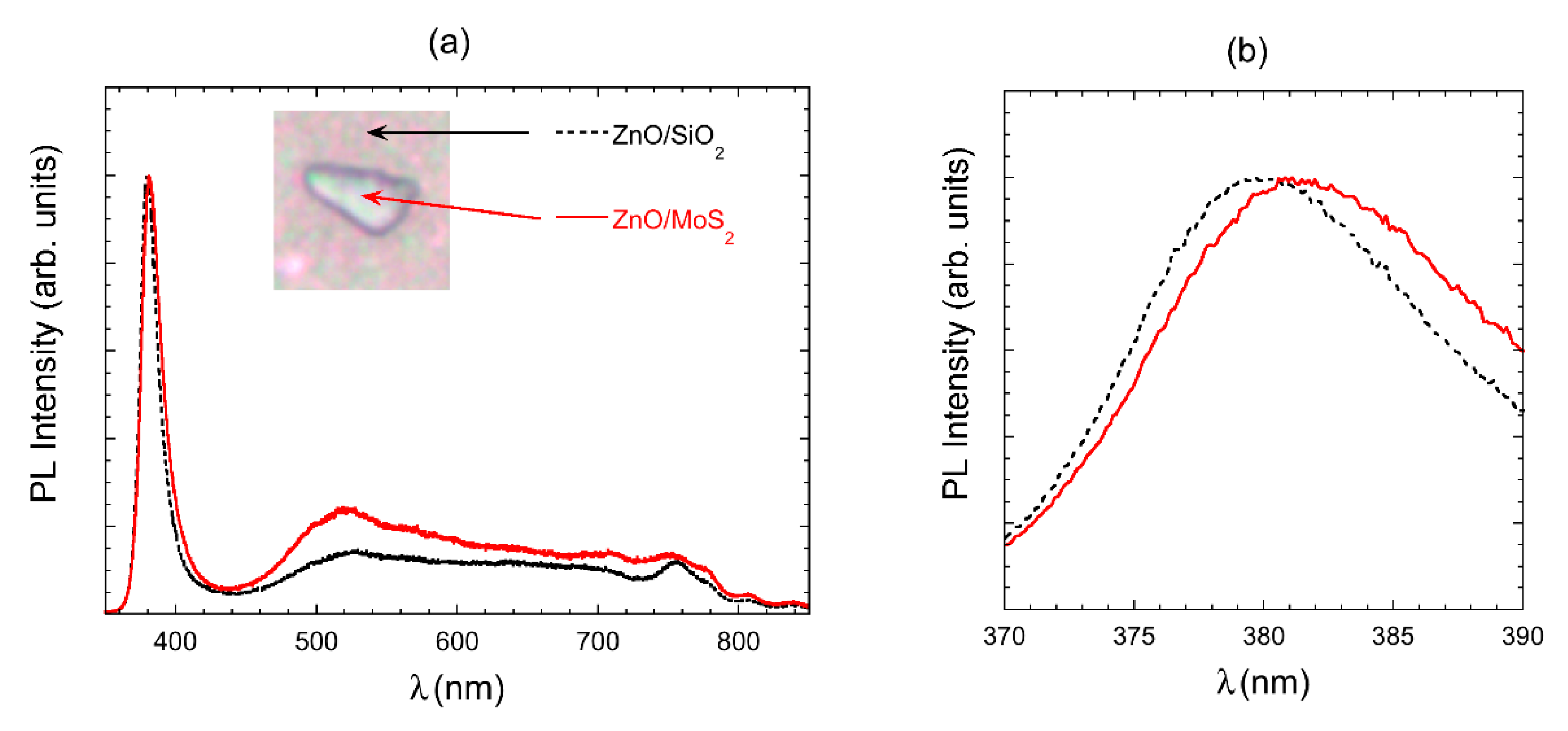
The truncated scalene triangle shown in Figure 3g was mapped and observed under the optical microscope: its sides are 4.8, 7.8, and 8 μm in length. Afterward, we investigated the PL spectra for ZnO nanorods deposited on MoS2 and SiO2, with reference to the scalene triangle reported in Figure 3g. Figure 5a shows the PL spectra and their position, acquired through a 50X objective. The two spectra were normalized in the plot.
The continuous wave PL spectrum of ZnO NWs was acquired at room temperature, so it is not possible to obtain a better resolution of different emission bands. Although the ZnO deposition temperature was quite low, the observed PL spectrum, reported in Figure 5a, is similar to the ones reported in the literature: we fitted near band emission (NBE) in the UV and defect emission (DE) in the visible with Gaussian functions using two peaks, which are centered at 377.7 and 384.9 nm for NBE. NBE is assigned to exciton emission, while visible emission strongly depends on the growth procedure and is assigned to defect emission. In our case, a broadband extends from 500 to 700 nm. The peak around 760 nm is a second-order peak of the NBE emission.
The ZnO grown on the MoS2 flake shows higher DE emission, which could be ascribed to a lower crystalline quality of the ZnO nanorods when they grow on the MoS2 flake. It is also possible to see in Figure 5b that NBE peak for ZnO/MoS2 is red-shifted (Gaussian peaks used for the fit are centered at 380.0 and 390.0 nm)) compared to the NBE peak of ZnO/SiO2, due to a lower mean diameter of the nanorods grown on SiO2 with respect to that grown on MoS2.
3.3. Functional Characterization
When developing gas sensing devices, it is strategic to determine which regions or interfaces of the device are mostly responsible for the overall response and for the drift. For example, in semiconducting oxide DC conductivity, one would like to separate the intragrain from the intergrain contribution and both from the metal-semiconductor junction, a task which is very difficult to accomplish through impedance and four-point probe measurements [44]. Optical measurements, in addition to avoiding the issues related to metal contacts, can be effectively employed to identify the MoS2 active regions of a sample, limited only by diffraction, gaining knowledge useful to electric gas sensing as well.
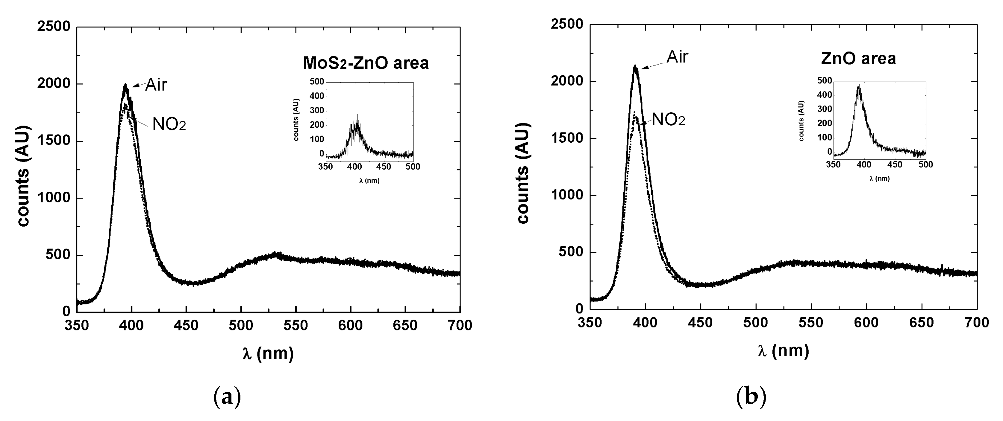
The temperature of the fabricated device was set to 200 °C, in order to operate in a temperature range where reversible chemisorption of NO2 takes place. Constant airflow flew into the test chamber for half an hour, then NO2 diluted in dry air was introduced in the test chamber, until a steady state PL signal was observed. Afterward, dry airflow was restored until the recovery of the baseline signal was obtained. Quenching of continuous-wave photoluminescence (CWPL) spectra due to interaction with 10ppm NO2 is shown in Figure 6 for two points: one located inside the MoS2-ZnO structure reported in Figure 5a and the other immediately outside on the ZnO. Quenching is visible mostly on the UV peak, which is ascribable to the ZnO NWs, while no appreciable change in the visible part of the PL spectrum is detected.
Setting as a feature the area under exciton (UV) peak (from 380 to 410nm) over the wavelength interval, the values reported in Table 2. can be extracted. The relative change of the chosen feature was indeed appreciably higher for the region where pure ZnO is grown, ascribable to the smaller size of the NW in the ZnO region compared to the MoS2+ZnO region.
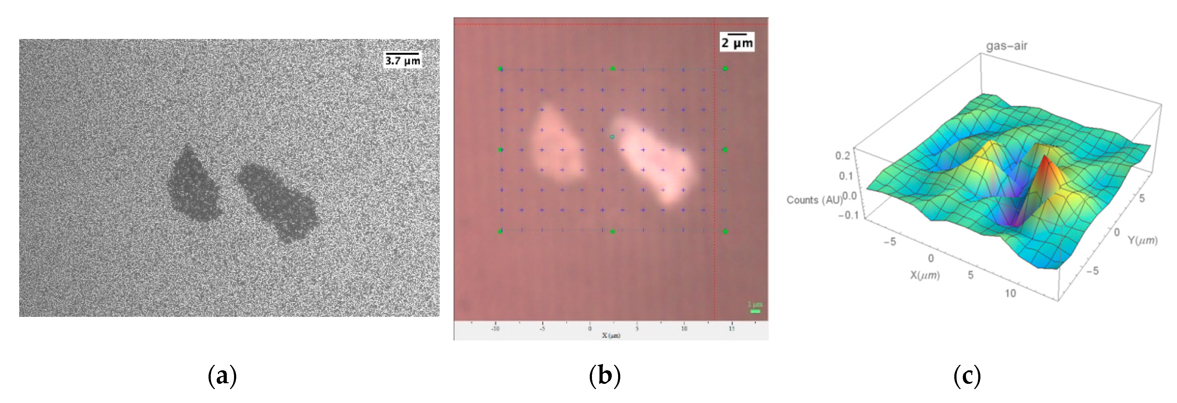
In order to increase the contribution of MoS2, which in Figure 3g is buried under the ZnO and therefore does not come into contact with surrounding gaseous species, we investigated a border region of the sample where the ZnO deposition by shadow mask sputtering was less effective and a lower density of the NWs is obtained, leaving the underlying MoS2 flakes in part uncovered. Figure 7c reports the bi-dimensional mapping of the relative change of the integral exciton (UV) peak (from 380 to 410 nm) PL emission for the structure made by two MoS2 flakes closed to the border over which ZnO was deposited, whose SEM image is reported in Figure 7a. Differently from the results reported in Figure 6, where a better optical gas sensing response is obtained for the bare ZnO area, when the ZnO NWs density is lower, and the gaseous species interact with the MoS2 flakes, the response is higher in the region where the ZnO NWs are coupled to the MoS2 flakes (Figure 7c), confirming the hypothesis of the synergic response induced by coupling the 2D to the 1D material.
4. Conclusions
We demonstrated the feasibility of depositing by magnetron sputtering vertically aligned 1D ZnO nanorods on 2D MoS2 flakes obtained by exfoliation, preserving the structure of the 2D material. The PL optical properties of the hybrid structure were assessed towards developing a contactless optical chemical sensor, and we made a first attempt to use PL imaging spectroscopy to investigate sensing applications of a hybrid 1D/2D structure. Since NO2 quenches the PL signal without shifting the peak, as long as issues related to cross sensitivities, to interfering species and humidity are addressed, and signal power is improved, a portable sensor can be realized in principle using a photodiode as a detector, and a LED as photoexcitation source.
Author Contributions
Conceptualisation: M.D. and F.R.; Investigation, G.F., M.F., T.T.L.D.; M.D., F.R. and C.B.; Supervision, C.B. All authors have read and agreed to the published version of the manuscript.
Funding
The NATO Science partially funded the research leading to these results for Peace and Security Programme under grant N° 9085043, “NANEOS—Multi-sensor system for rapid detection of dangerous and hazardous agents”, and Regional Funding - Project CYBERSORT.
Conflicts of Interest
The authors declare no conflict of interest.
References
- Liao, L.; Lin, Y.C.; Bao, M.Q.; Cheng, R.; Bai, J.W.; Liu, Y.A.; Qu, Y.Q.; Wang, K.L.; Huang, Y.; Duan, X.F. High-speed graphene transistors with a self-aligned nanowire gate. Nature 2010, 467, 305–308. [Google Scholar] [CrossRef] [PubMed]
- Han, F.; Yang, S.M.; Jing, W.X.; Jiang, K.; Jiang, Z.D.; Liu, H.; Li, L. Surface plasmon enhanced photoluminescence of ZnO nanorods by capping reduced graphene oxide sheets. Opt. Express 2014, 22, 11436–11445. [Google Scholar] [CrossRef] [PubMed]
- Liu, R.; Fu, X.W.; Meng, J.; Bie, Y.Q.; Yu, D.P.; Liao, Z.M. Graphene plasmon enhanced photoluminescence in ZnO microwires. Nanoscale 2013, 5, 5294–5298. [Google Scholar] [CrossRef] [PubMed]
- Zhang, S.G.; Wen, L.; Li, J.L.; Gao, F.L.; Zhang, X.W.; Li, L.H.; Li, G.Q. Plasmon-enhanced ultraviolet photoluminescence from highly ordered ZnO nanorods/graphene hybrid structure decorated with Au nanospheres. J. Phys. D Appl. Phys. 2014, 47. [Google Scholar] [CrossRef]
- Hwang, S.W.; Shin, D.H.; Kim, C.O.; Hong, S.H.; Kim, M.C.; Kim, J.; Lim, K.Y.; Kim, S.; Choi, S.H.; Ahn, K.J.; et al. Plasmon-Enhanced Ultraviolet Photoluminescence from Hybrid Structures of Graphene/ZnO Films. Phys. Rev. Lett. 2010, 105. [Google Scholar] [CrossRef]
- Ahn, K.J.; Hwang, S.W.; Shin, D.H.; Kim, C.O.; Hong, S.H.; Kim, M.C.; Kim, J.; Lim, K.Y.; Kim, S.; Choi, S.H.; et al. Comment on “Plasmon-Enhanced Ultraviolet Photoluminescence from Hybrid Structures of Graphene/ZnO Films” Reply. Phys. Rev. Lett. 2011, 107. [Google Scholar] [CrossRef]
- Wang, Q.H.; Kalantar-Zadeh, K.; Kis, A.; Coleman, J.N.; Strano, M.S. Electronics and optoelectronics of two-dimensional transition metal dichalcogenides. Nat. Nanotechnol. 2012, 7, 699–712. [Google Scholar] [CrossRef]
- Yi, M.; Shen, Z.G. A review on mechanical exfoliation for the scalable production of graphene. J. Mater. Chem. A 2015, 3, 11700–11715. [Google Scholar] [CrossRef]
- Ottaviano, L.; Palleschi, S.; Perrozzi, F.; D’Olimpio, G.; Priante, F.; Donarelli, M.; Benassi, P.; Nardone, M.; Gonchigsuren, M.; Gombosuren, M.; et al. Mechanical exfoliation and layer number identification of MoS2 revisited. 2D Mater. 2017, 4. [Google Scholar] [CrossRef]
- Radisavljevic, B.; Radenovic, A.; Brivio, J.; Giacometti, V.; Kis, A. Single-layer MoS2 transistors. Nat. Nanotechnol. 2011, 6, 147–150. [Google Scholar] [CrossRef]
- Donarelli, M.; Prezioso, S.; Perrozzi, F.; Bisti, F.; Nardone, M.; Giancaterini, L.; Cantalini, C.; Ottaviano, L. Response to NO2 and other gases of resistive chemically exfoliated MoS2-based gas sensors. Sens. Actuat B Chem. 2015, 207, 602–613. [Google Scholar] [CrossRef]
- Perkins, F.K.; Friedman, A.L.; Cobas, E.; Campbell, P.M.; Jernigan, G.G.; Jonker, B.T. Chemical Vapor Sensing with Mono layer MoS2. Nano Lett. 2013, 13, 668–673. [Google Scholar] [CrossRef] [PubMed]
- Cho, B.; Hahm, M.G.; Choi, M.; Yoon, J.; Kim, A.R.; Lee, Y.J.; Park, S.G.; Kwon, J.D.; Kim, C.S.; Song, M.; et al. Charge-transfer-based Gas Sensing Using Atomic-layer MoS2. Sci. Rep. UK 2015, 5. [Google Scholar] [CrossRef] [PubMed]
- Li, H.; Yin, Z.Y.; He, Q.Y.; Li, H.; Huang, X.; Lu, G.; Fam, D.W.H.; Tok, A.I.Y.; Zhang, Q.; Zhang, H. Fabrication of Single- and Multilayer MoS2 Film-Based Field-Effect Transistors for Sensing NO at Room Temperature. Small 2012, 8, 63–67. [Google Scholar] [CrossRef]
- Samnakay, R.; Jiang, C.; Rumyantsev, S.L.; Shur, M.S.; Balandin, A.A. Selective chemical vapor sensing with few-layer MoS2 thin-film transistors: Comparison with graphene devices. Appl. Phys. Lett. 2015, 106. [Google Scholar] [CrossRef] [Green Version]
- Schedin, F.; Geim, A.K.; Morozov, S.V.; Hill, E.W.; Blake, P.; Katsnelson, M.I.; Novoselov, K.S. Detection of individual gas molecules adsorbed on graphene. Nat. Mater. 2007, 6, 652–655. [Google Scholar] [CrossRef]
- Djurisic, A.B.; Leung, Y.H. Optical properties of ZnO nanostructures. Small 2006, 2, 944–961. [Google Scholar] [CrossRef]
- Vanheusden, K.; Warren, W.L.; Seager, C.H.; Tallant, D.R.; Voigt, J.A.; Gnade, B.E. Mechanisms behind green photoluminescence in ZnO phosphor powders. J. Appl. Phys. 1996, 79, 7983–7990. [Google Scholar] [CrossRef]
- Hu, J.Q.; Bando, Y. Growth and optical properties of single-crystal tubular ZnO whiskers. Appl. Phys. Lett. 2003, 82, 1401–1403. [Google Scholar] [CrossRef]
- Lin, B.X.; Fu, Z.X.; Jia, Y.B. Green luminescent center in undoped zinc oxide films deposited on silicon substrates. Appl. Phys. Lett. 2001, 79, 943–945. [Google Scholar] [CrossRef]
- Studenikin, S.A.; Cocivera, M. Time-resolved luminescence and photoconductivity of polycrystalline ZnO films. J. Appl. Phys. 2002, 91, 5060–5065. [Google Scholar] [CrossRef]
- Yao, B.D.; Chan, Y.F.; Wang, N. Formation of ZnO nanostructures by a simple way of thermal evaporation. Appl. Phys. Lett. 2002, 81, 757–759. [Google Scholar] [CrossRef]
- Roy, V.A.L.; Djurisic, A.B.; Chan, W.K.; Gao, J.; Lui, H.F.; Surya, C. Luminescent and structural properties of ZnO nanorods prepared under different conditions. Appl. Phys. Lett. 2003, 83, 141–143. [Google Scholar] [CrossRef] [Green Version]
- Faglia, G.; Baratto, C.; Sberveglieri, G.; Zha, M.; Zappettini, A. Adsorption effects of NO2 at ppm level on visible photoluminescence response of SnO2 nanobelts. Appl. Phys. Lett. 2005, 86. [Google Scholar] [CrossRef]
- Comini, E.; Baratto, C.; Faglia, G.; Ferroni, M.; Sberveglieri, G. Single crystal ZnO nanowires as optical and conductometric chemical sensor. J. Phys. D Appl. Phys. 2007, 40, 7255–7259. [Google Scholar] [CrossRef]
- Baratto, C.; Todros, S.; Faglia, G.; Comini, E.; Sberveglieri, G.; Lettieri, S.; Santamaria, L.; Maddalena, P. Luminescence response of ZnO nanowires to gas adsorption. Sens. Actuat B Chem. 2009, 140, 461–466. [Google Scholar] [CrossRef]
- Chen, L.B.; Xue, F.; Li, X.H.; Huang, X.; Wang, L.F.; Kou, J.Z.; Wang, Z.L. Strain-Gated Field Effect Transistor of a MoS2 ZnO 2D-1D Hybrid Structure. ACS Nano 2016, 10, 1546–1551. [Google Scholar] [CrossRef]
- Li, H.X.; Dong, W.; Zhang, J.; Xi, J.H.; Du, G.; Ji, Z.G. MoS2 nanosheet/ZnO nanowire hybrid nanostructures for photoelectrochemical water splitting. J. Am. Ceram. Soc. 2018, 101, 3989–3996. [Google Scholar] [CrossRef]
- Zhang, K.N.; Zhang, Y.; Zhang, T.N.; Dong, W.J.; Wei, T.X.; Sun, Y.; Chen, X.; Shen, G.Z.; Dai, N. Vertically coupled ZnO nanorods on MoS2 monolayers with enhanced Raman and photoluminescence emission. Nano Res. 2015, 8, 743–750. [Google Scholar] [CrossRef] [Green Version]
- Zhao, S.F.; Wang, G.J.; Liao, J.C.; Lv, S.S.; Zhu, Z.N.; Li, Z.C. Vertically aligned MoS2/ZnO nanowires nanostructures with highly enhanced NO2 sensing activities. Appl. Surf. Sci. 2018, 456, 808–816. [Google Scholar] [CrossRef]
- Zhou, Y.; Gao, C.; Guo, Y.C. UV assisted ultrasensitive trace NO2 gas sensing based on few-layer MoS2 nanosheet-ZnO nanowire heterojunctions at room temperature. J. Mater. Chem. A 2018, 6, 10286–10296. [Google Scholar] [CrossRef]
- Yang, T.; Chen, M.J.; Kong, Q.Q.; Luo, X.L.; Jiao, K. Toward DNA electrochemical sensing by free-standing ZnO nanosheets grown on 2D thin-layered MoS2. Biosens. Bioelectron. 2017, 89, 538–544. [Google Scholar] [CrossRef] [PubMed]
- Chacko, L.; Poyyakkara, A.; Kumar, V.B.S.; Aneesh, P.M. MoS2-ZnO nanocomposites as highly functional agents for anti-angiogenic and anti-cancer theranostics. J. Mater. Chem. B 2018, 6, 3048–3057. [Google Scholar] [CrossRef]
- Baratto, C. Growth and properties of ZnO nanorods by RF-sputtering for detection of toxic gases. RSC Adv. 2018, 8, 32038–32043. [Google Scholar] [CrossRef] [Green Version]
- Benameur, M.M.; Radisavljevic, B.; Heron, J.S.; Sahoo, S.; Berger, H.; Kis, A. Visibility of dichalcogenide nanolayers. Nanotechnology 2011, 22. [Google Scholar] [CrossRef]
- Donarelli, M.; Bisti, F.; Perrozzi, F.; Ottaviano, L. Tunable sulfur desorption in exfoliated MoS2 by means of thermal annealing in ultra-high vacuum. Chem. Phys. Lett. 2013, 588, 198–202. [Google Scholar] [CrossRef]
- Syari’ati, A.; Kumar, S.; Zahid, A.; El Yumin, A.A.; Ye, J.T.; Rudolf, P. Photoemission spectroscopy study of structural defects in molybdenum disulfide (MoS2) grown by chemical vapor deposition (CVD). Chem. Commun. 2019, 55, 10384–10387. [Google Scholar] [CrossRef] [Green Version]
- Chen, M.T.; Ting, J.M. Sputter deposition of ZnO nanorods/thin-film structures on Si. Thin Solid Films 2006, 494, 250–254. [Google Scholar] [CrossRef]
- Baratto, C.; Ferroni, M.; Comini, E.; Faglia, G.; Kaciulis, S.; Balijepalli, S.K.; Sberveglieri, G. Vapour phase nucleation of ZnO nanowires on GaN: Growth habit, interface study and optical properties. RSC Adv. 2016, 6, 15087–15093. [Google Scholar] [CrossRef]
- Bertrand, P.A. SURFACE-PHONON DISPERSION OF MOS2. Phys. Rev. B 1991, 44, 5745–5749. [Google Scholar] [CrossRef]
- Valerius, P.; Kretschmer, S.; Senkovskiy, B.V.; Wu, S.L.; Hall, J.; Herman, A.; Ehlen, N.; Ghorbani-Asl, M.; Gruneis, A.; Krasheninnikov, A.V.; et al. Reversible crystalline-to-amorphous phase transformation in monolayer MoS2 under grazing ion irradiation. 2D Mater. 2020, 7. [Google Scholar] [CrossRef]
- Zhu, J.Q.; Wang, Z.C.; Yu, H.; Li, N.; Zhang, J.; Meng, J.L.; Liao, M.Z.; Zhao, J.; Lu, X.B.; Du, L.J.; et al. Argon Plasma Induced Phase Transition in Monolayer MoS2. J. Am. Chem. Soc. 2017, 139, 10216–10219. [Google Scholar] [CrossRef] [PubMed]
- Russo, V.; Ghidelli, M.; Gondoni, P.; Casari, C.S.; Bassi, A.L. Multi-wavelength Raman scattering of nanostructured Al-doped zinc oxide. J. Appl. Phys. 2014, 115. [Google Scholar] [CrossRef] [Green Version]
- Barsan, N.; Weimar, U. Understanding the fundamental principles of metal oxide based gas sensors; the example of CO sensing with SnO2 sensors in the presence of humidity. J. Phys. Condens. Mat. 2003, 15, R813–R839. [Google Scholar] [CrossRef]
Figure 1.
Sketch of the deposition steps.

Figure 2.
Sketch of the experimental setup.

Figure 3.
(a) Exfoliated MoS2; from (b) to (h) ZnO+MoS2 with the following deposition conditions: (b) T = 200 °C—5 min, 200 W, no catalyzer; (c)T = 200 °C—5 min, 200 W, Sn catalyzer; (d) T = 250 °C—5 min, 200 W, Sn catalyzer; (e) T = 250 °C—5 min, 150 W, Sn catalyzer; (f) T = 250 °C—5 min, 100 W, Sn catalyzer; (g) T = 250 °C—10 min, 100 W, Sn catalyzer; (h) T = 250 °C—15 min, 100 W, Sn catalyzer.

Figure 4.
(a) Raman spectrum of the triangular MoS2 flake reported in Figure 3a; (b) Raman spectrum of a ZnO/MoS2 sample G prepared as reported in Table 1; (c) Raman spectrum of the ZnO nanorods of sample G.

Figure 5.
(a) Photoluminescence (PL) comparison of ZnO growth over MoS2 and ZnO over SiO2. The inset reports the optical image of the scalene triangle, with the position of spectra acquisition. (b) Close up image of the near band emission (NBE).
Figure 5.
(a) Photoluminescence (PL) comparison of ZnO growth over MoS2 and ZnO over SiO2. The inset reports the optical image of the scalene triangle, with the position of spectra acquisition. (b) Close up image of the near band emission (NBE).

Figure 6.
(a) Response to 10ppm NO2 in dry air at 200 degC inside the MoS2-ZnO structure reported in Figure 5 and (b) immediately outside on the ZnO. Insets report the difference of the signals.
Figure 6.
(a) Response to 10ppm NO2 in dry air at 200 degC inside the MoS2-ZnO structure reported in Figure 5 and (b) immediately outside on the ZnO. Insets report the difference of the signals.

Figure 7.
(a) SEM and (b) optical image of two MoS2+ZnO flakes whose PL response to 3ppm of NO2 at T = 200 °C has been mapped on every reported cross (c) bidimensional mapping of the relative change in the exciton (UV) peak (from 380 to 410 nm) PL emission at T = 200 °C, 30% r.h., NO2 3 ppm.
Figure 7.
(a) SEM and (b) optical image of two MoS2+ZnO flakes whose PL response to 3ppm of NO2 at T = 200 °C has been mapped on every reported cross (c) bidimensional mapping of the relative change in the exciton (UV) peak (from 380 to 410 nm) PL emission at T = 200 °C, 30% r.h., NO2 3 ppm.


Table 1.
Deposition parameters for ZnO samples. Sample name refers to Figure 3b–h images.
Table 1.
Deposition parameters for ZnO samples. Sample name refers to Figure 3b–h images.
| Sample Name | Substrate Temperature (°C) | Deposition Time (minutes) | Power (W) | Sn Catalyzer |
|---|---|---|---|---|
| B | 200 | 5 | 200 | No |
| C | 200 | 5 | 200 | Yes |
| D | 250 | 5 | 200 | Yes |
| E | 250 | 5 | 150 | Yes |
| F | 250 | 5 | 100 | Yes |
| G | 250 | 10 | 100 | Yes |
| H | 250 | 15 | 100 | Yes |
Table 2.
Value of PL as peak area (from 380 nm to 410 nm) in air and in 10 ppm of NO2 and corresponding response (relative change of peak area) over the MoS2 sheet+ZnO NWs region in Figure 5 and immediately outside over the ZnO NWs.
Table 2.
Value of PL as peak area (from 380 nm to 410 nm) in air and in 10 ppm of NO2 and corresponding response (relative change of peak area) over the MoS2 sheet+ZnO NWs region in Figure 5 and immediately outside over the ZnO NWs.
| MoS2 Sheet+ ZnO NWs | ZnO NWs | |
|---|---|---|
| Air | 12,300 | 12,100 |
| 10ppm of NO2 | 11,260 | 9700 |
| Response | 9% | 25% |
© 2020 by the authors. Licensee MDPI, Basel, Switzerland. This article is an open access article distributed under the terms and conditions of the Creative Commons Attribution (CC BY) license (http://creativecommons.org/licenses/by/4.0/).
Share and Cite
MDPI and ACS Style
Faglia, G.; Ferroni, M.; Dang, T.T.L.; Donarelli, M.; Rigoni, F.; Baratto, C. Vertically Coupling ZnO Nanorods onto MoS2 Flakes for Optical Gas Sensing. Chemosensors 2020, 8, 19. https://doi.org/10.3390/chemosensors8010019
AMA Style
Faglia G, Ferroni M, Dang TTL, Donarelli M, Rigoni F, Baratto C. Vertically Coupling ZnO Nanorods onto MoS2 Flakes for Optical Gas Sensing. Chemosensors. 2020; 8(1):19. https://doi.org/10.3390/chemosensors8010019
Chicago/Turabian StyleFaglia, Guido, Matteo Ferroni, Thi Thanh Le Dang, Maurizio Donarelli, Federica Rigoni, and Camilla Baratto. 2020. "Vertically Coupling ZnO Nanorods onto MoS2 Flakes for Optical Gas Sensing" Chemosensors 8, no. 1: 19. https://doi.org/10.3390/chemosensors8010019
Note that from the first issue of 2016, this journal uses article numbers instead of page numbers. See further details here.