
The DEPFET Sensor-Amplifier Structure: A Method to Beat 1/f Noise and Reach Sub-Electron Noise in Pixel Detectors


Abstract
:
1. Introduction
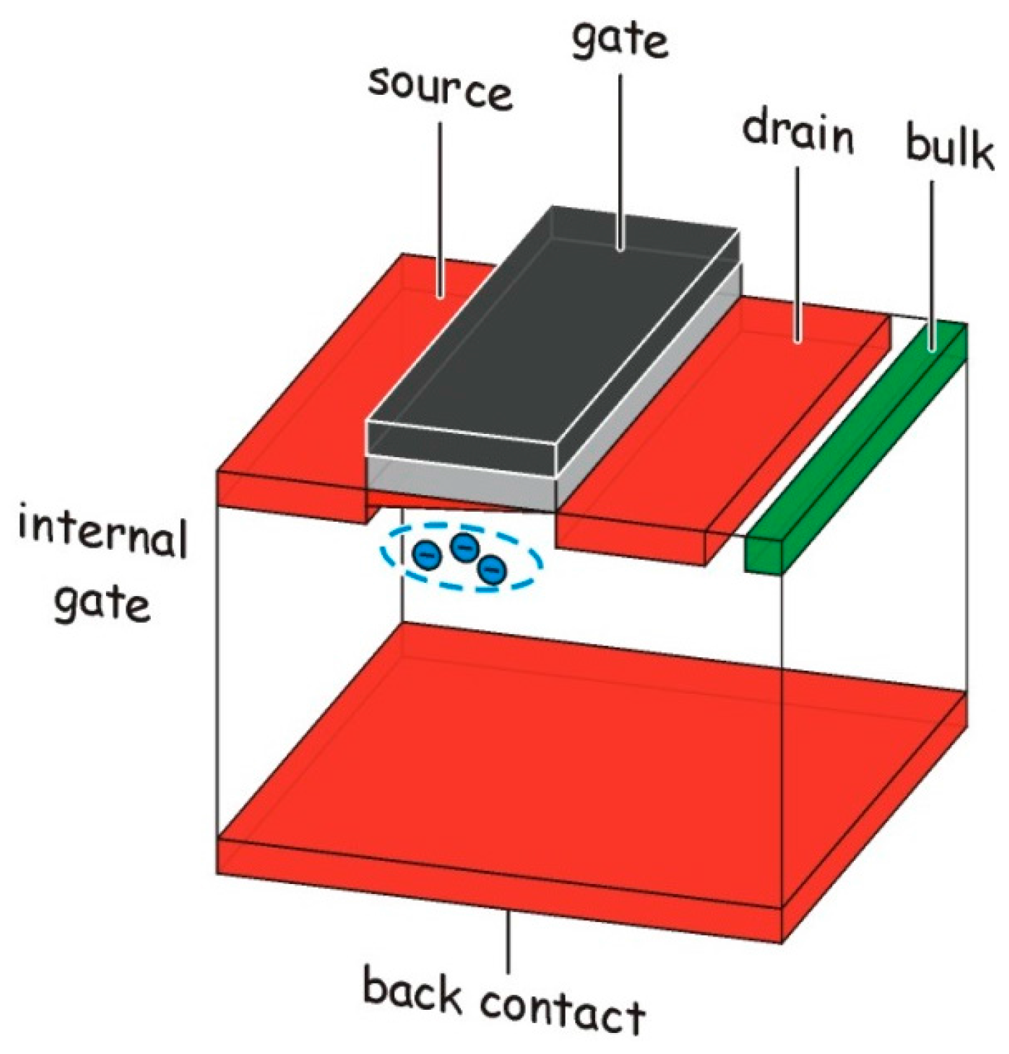
2. The Depleted p-Channel MOSFET (DEPFET)—A Detector-Amplifier Structure
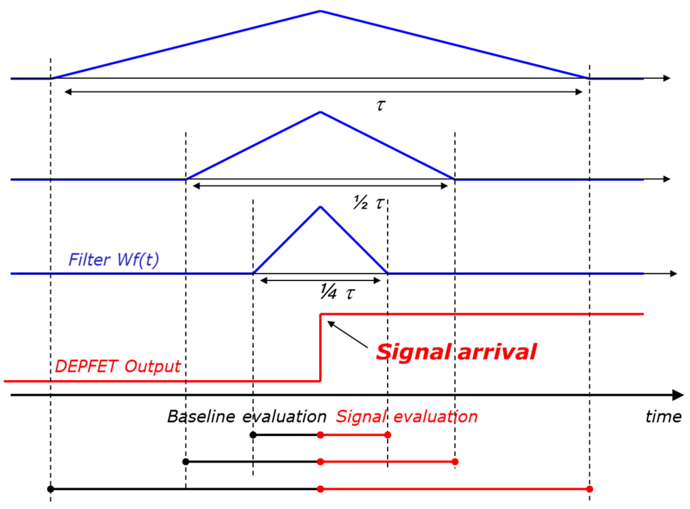
3. DEPFET Readout
- •
- Baseline
- •
- Baseline + Signal
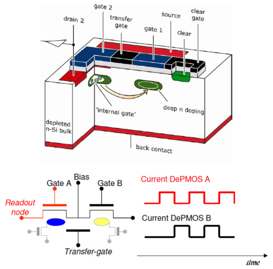
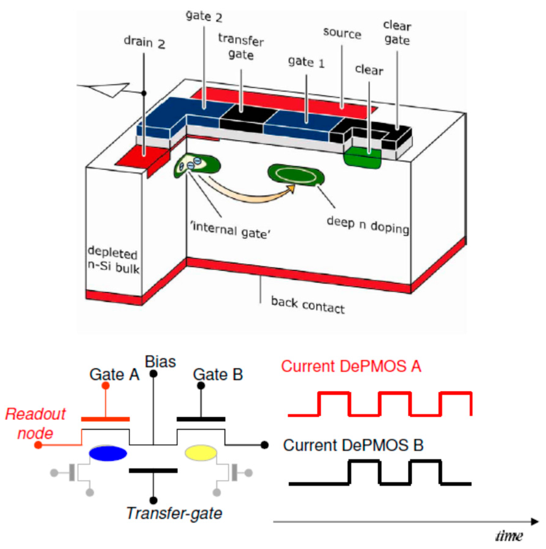
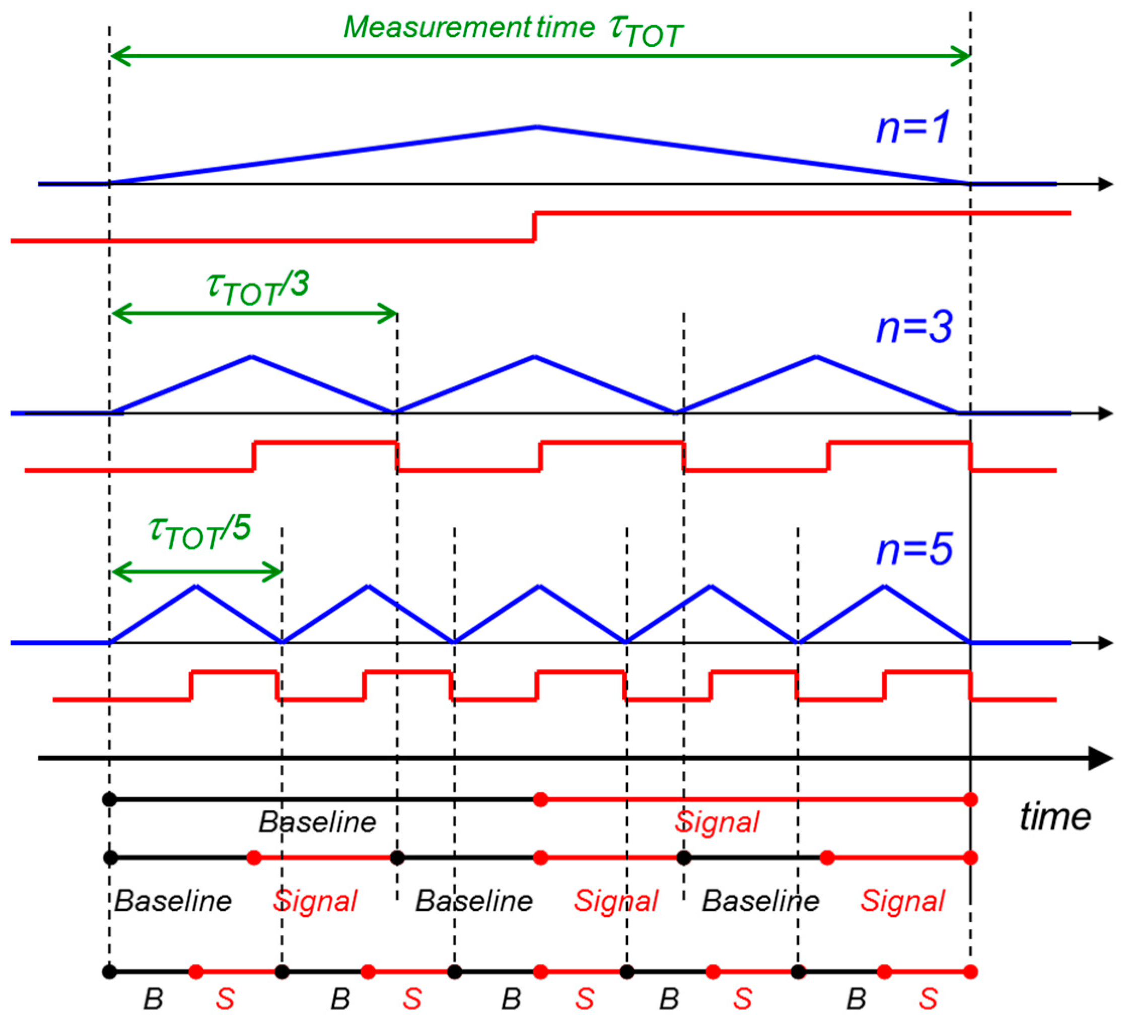
4. RNDR-DEPFET
5. DEPFET Noise Analysis
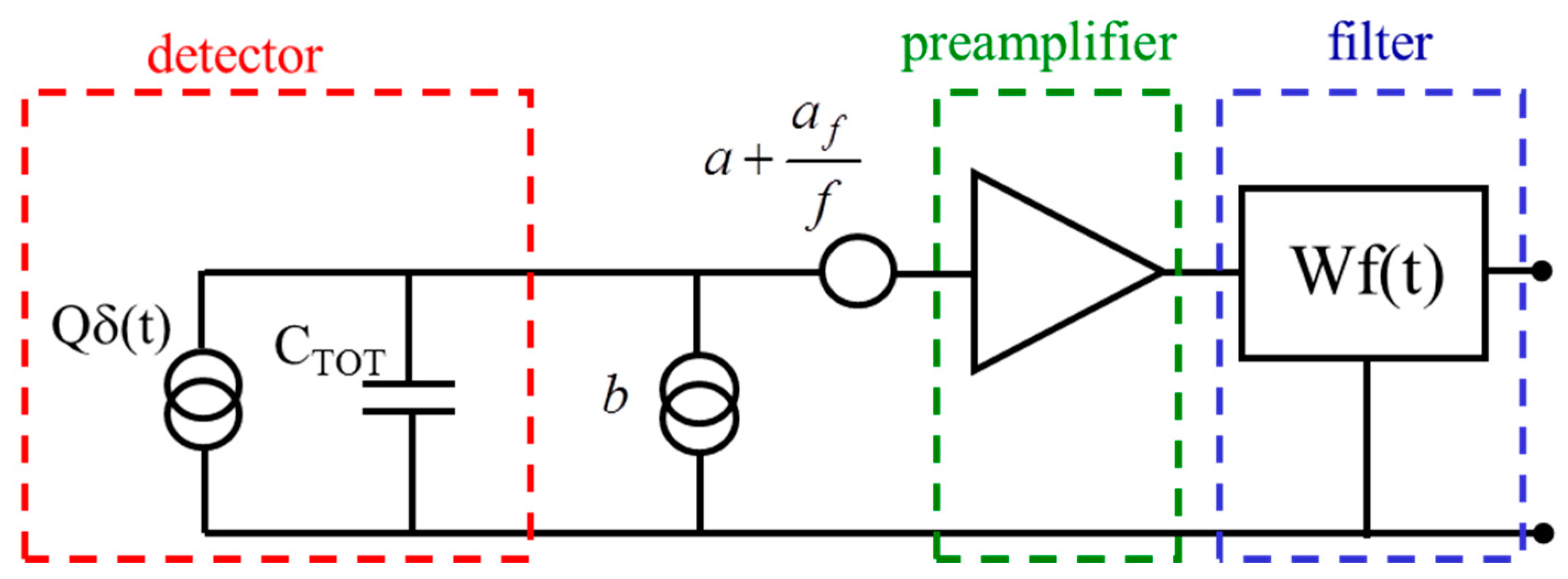
5.1. Noise in Single Readout
- •
- CTOT is the equivalent input capacitance of the system.
- •
- a, af and b are the series white, the series 1/f and the parallel white physical noise sources, referred to the input.
- •
- A1, A2 and A3 are the filter parameters. They depend on the shape of the weighting function Wf(t) implemented by the readout electronics.
- •
- τ is the shaping time of the readout filter and is an expression of the time needed to perform one measurement.
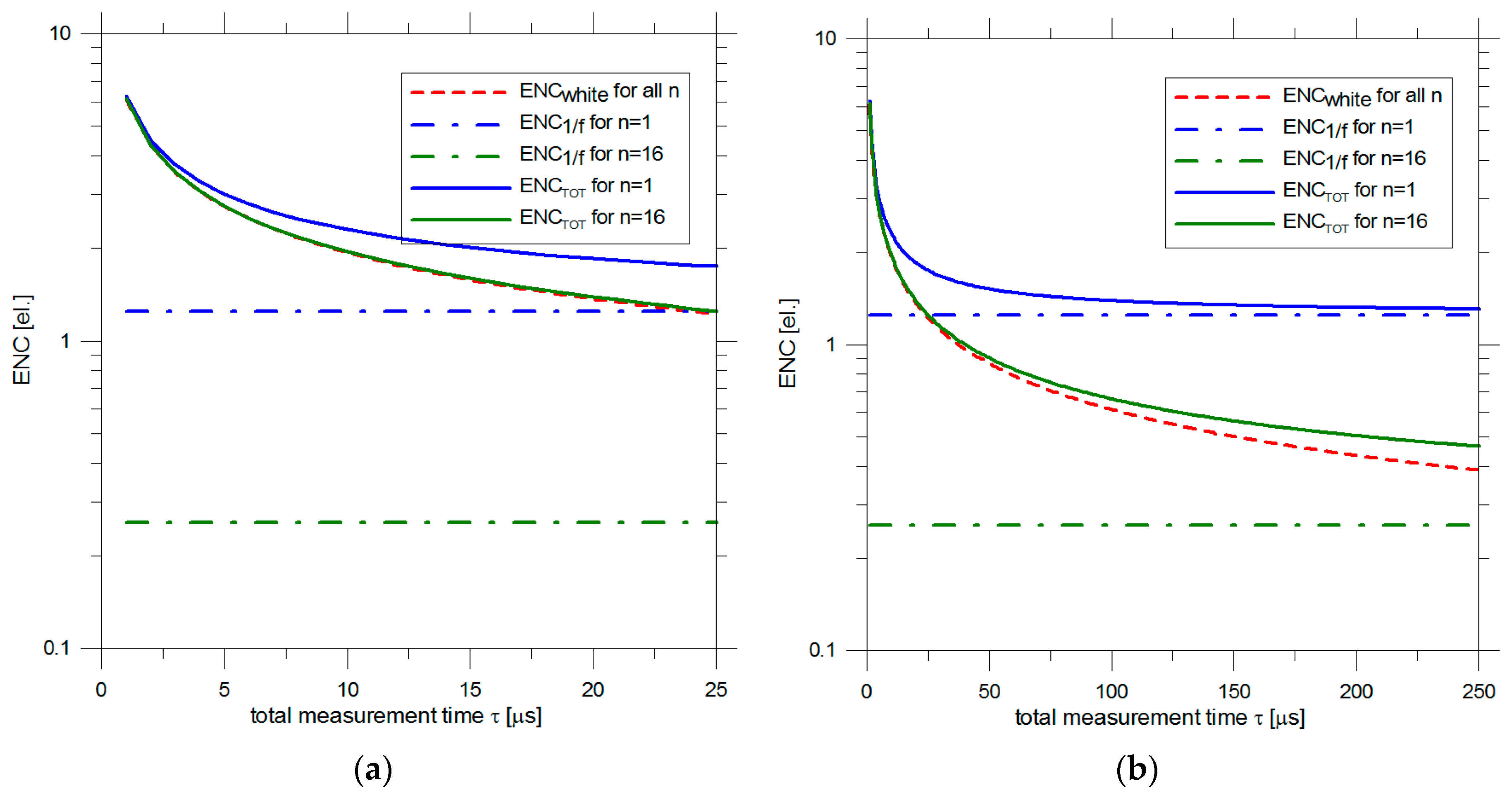
5.2. Noise in Repetitive Non-Destructive Readout
- •
- is independent from the number of measurements n
- •
- scales approximately as 1/n
- •
- the white series noise and the 1/f series noise contributions scale as 1/n
- •
- the noise due to the leakage current that fills the internal gate increases with n, i.e., with the total measurement time.
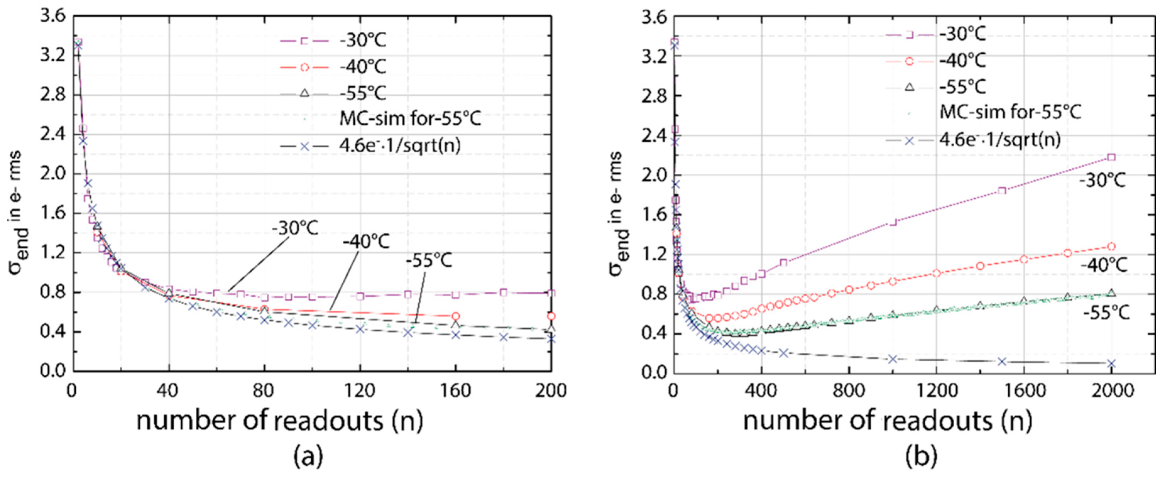
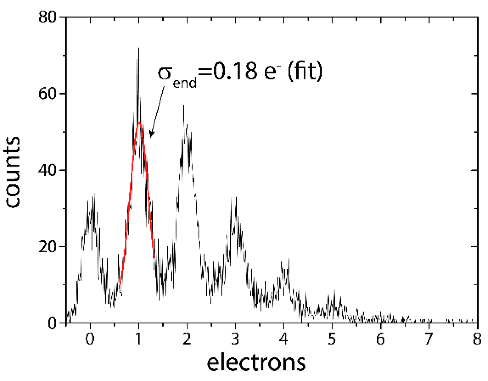
6. Experimental Evidence
7. Summary and Outlook
Acknowledgments
Author Contributions
Conflicts of Interest
References
- Hartmann, R.; Stephan, K.-H.; Strüder, L. The quantum efficiency of pn-detectors from the near infrared to the soft X-ray region. Nucl. Instrum. Methods Phys. Res. Sect. A 2000, 439, 216–220. [Google Scholar] [CrossRef]
- Kraft, R.P.; Burrows, D.N.; Garmire, G.P.; Nousek, J.A.; Janesick, J.R.; Vu, P.N. Soft X-ray spectroscopy with sub-electron readnoise charge-coupled devices. Nucl. Instrum. Methods Phys. Res. Sect. A 1995, 361, 372–383. [Google Scholar] [CrossRef]
- Kemmer, J.; Lutz, G. New semiconductor detector concepts. Nucl. Instr. Meth. A 1987, 253, 365–377. [Google Scholar] [CrossRef]
- Lutz, G.; Herrmann, S.; Lechner, P.; Porro, M.; Richter, R.H.; Strüder, L.; Treis, J. New DEPFET structures, concepts, simulations and experimental results. Proc. SPIE 2008, 7021. [Google Scholar] [CrossRef]
- Gatti, E.; Rehak, P. Semiconductor drift chamber—An application of a novel charge transport scheme. Nucl. Instrum. Methods Phys. Res. Sect. A 1984, 225, 608–621. [Google Scholar] [CrossRef]
- Kemmer, J.; Lutz, G. Low capacitive drift diode. Nucl. Instr. Meth. A 1987, 253, 378–381. [Google Scholar] [CrossRef]
- Lutz, G. Halbleiterdetektor Mit Einem Zwischenspeicher für Signalladungsträger und Entsprechendes Betriebsverfahren. DE Patent 102011115656 A1, 28 March 2013. (In Germay)[Google Scholar]
- Wölfel, S.; Herrmann, S.; Lechner, P.; Lutz, G.; Porro, M.; Richter, R.H.; Strüder, L.; Treis, J. A Novel Way of Single Optical Photon Detection: Beating the 1/f Noise Limit with Ultra High Resolution DEPFET-RNDR Devices. IEEE Trans. Nucl. Sci. 2007, 54, 1311–1318. [Google Scholar] [CrossRef]
- Porro, M.; Herrmann, S.; Hörnel, N. Multi correlated double sampling with exponential reset. In Nuclear Science Symposium Conference Record, Proceedings of the IEEE NSS’07, Honolulu, HI, USA, 26 October–3 November 2007; pp. 291–298.
- Porro, M.; de Vita, G.; Herrmann, S.; Lauf, T.; Treis, J.; Wassatsch, A.; Bombelli, L.; Fiorini, C. ASTEROID: A 64 channel ASIC for source follower readout of DEPFET arrays for X-ray astronomy. Nucl. Instr. Meth. Phys. Res. Sect. A 2010, 617, 351–357. [Google Scholar] [CrossRef]
- Porro, M.; Bianchi, D.; De Vita, G.; Hartmann, R.; Hauser, G.; Herrmann, S.; Strüder, L.; Wassatsch, A. VERITAS: A 128-channel ASIC for the readout of pnCCDs and DEPFET arrays for X-ray imaging, spectroscopy and XFEL applications. IEEE Trans. Nucl. Sci. 2013, 60, 446–455. [Google Scholar] [CrossRef]
- Wölfel, S.; Herrmann, S.; Lechner, P.; Lutz, G.; Porro, M.; Richter, R.; Strüder, L.; Treis, J. Sub-electron noise measurements on repetitive non-destructive readout devices. Nucl. Instr. Meth. Phys. Res. Sect. A 2006, 566, 536–539. [Google Scholar] [CrossRef]
- Gatti, E.; Manfredi, P.F.; Sampietro, M.; Speziali, V. Suboptimal filtering of 1/ƒ-noise in detector charge measurements. Nucl. Instr. Meth. Phys. Res. Sect. A 1990, 297, 467–478. [Google Scholar] [CrossRef]
- Gatti, E.; Manfredi, P.F. Processing the signals from solid-state-detector in elementary particle physics. Riv. Nuovo Cimento 1986, 9, 1–146. [Google Scholar] [CrossRef]
- Gatti, E.; Sampietro, M.; Manfredi, P.F. Optimum filters for detector charge measurements in presence of 1f noise. Nucl. Instr. Meth. Phys. Res. Sect. A 1990, 287, 513–520. [Google Scholar] [CrossRef]
- Gatti, E.; Geraci, A.; Guazzoni, C. Multiple read-out of signals in presence of arbitrary noises Optimum filters. Nucl. Instr. Meth. Phys. Res. Sect. A 1998, 417, 342–353. [Google Scholar] [CrossRef]
- Porro, M.; Ferrari, G.; Fischer, P.; Halker, O.; Harter, M.; Herrmann, S.; Hornel, N.; Kohrs, R.; Krueger, H.; Lechner, P.; et al. Spectroscopic performance of the DePMOS detector/amplifier device with respect to different filtering techniques and operating conditions. IEEE Trans Nucl. Sci. 2006, 53, 401–408. [Google Scholar] [CrossRef]
- Treis, L.; Andricek, F.; Aschauer, K.; Heinzinger, S.; Herrmann, M.; Hilchenbach, T.; Lauf, P.; Lechner, G.; Lutz, P.; Majewski, M.; et al. MIXS on BepiColombo and its DEPFET based focal plane instrumentation. Nucl. Instr. Meth. Phys. Res. Sect. A 2010, 624, 540–547. [Google Scholar] [CrossRef]
- Porro, M.; Andricek, L.; Aschauer, S.; Bayer, M.; Becker, J.; Bombelli, L.; Castoldi, A.; de Vita, G.; Diehl, I.; Erdinger, F.; et al. Development of the DEPFET Sensor with Signal Compression: A Large Format X-ray Imager with Mega-Frame Readout Capability for the European XFEL. IEEE Trans. Nucl. Sci. 2012, 59, 3339–3351. [Google Scholar] [CrossRef]
- Lutz, G.; Lechner, P.; Porro, M.; Strüder, L.; de Vita, G. DEPFET sensor with intrinsic signal compression developed for use at the XFEL free electron laser radiation source. Nucl. Instr. Meth. Phys. Res. Sect. A 2010, 624, 528–532. [Google Scholar] [CrossRef]


| Number of Readouts n | A2 | ENC1/f |
|---|---|---|
| 1 | 0.88254 | 1.25 |
| 2 | 0.38287 | 0.82 |
| 4 | 0.17038 | 0.55 |
| 8 | 0.07823 | 0.37 |
| 16 | 0.03695 | 0.25 |
| 32 | 0.01782 | 0.18 |
© 2016 by the authors; licensee MDPI, Basel, Switzerland. This article is an open access article distributed under the terms and conditions of the Creative Commons Attribution (CC-BY) license (http://creativecommons.org/licenses/by/4.0/).
Share and Cite
Lutz, G.; Porro, M.; Aschauer, S.; Wölfel, S.; Strüder, L. The DEPFET Sensor-Amplifier Structure: A Method to Beat 1/f Noise and Reach Sub-Electron Noise in Pixel Detectors. Sensors 2016, 16, 608. https://doi.org/10.3390/s16050608
Lutz G, Porro M, Aschauer S, Wölfel S, Strüder L. The DEPFET Sensor-Amplifier Structure: A Method to Beat 1/f Noise and Reach Sub-Electron Noise in Pixel Detectors. Sensors. 2016; 16(5):608. https://doi.org/10.3390/s16050608
Chicago/Turabian StyleLutz, Gerhard, Matteo Porro, Stefan Aschauer, Stefan Wölfel, and Lothar Strüder. 2016. "The DEPFET Sensor-Amplifier Structure: A Method to Beat 1/f Noise and Reach Sub-Electron Noise in Pixel Detectors" Sensors 16, no. 5: 608. https://doi.org/10.3390/s16050608